3d nand harc etch
Figure 234c shows the cross-section after staircase contact etch and hard-mask strip and clean. A-Carbon films are critical in the 3D NAND process.
3d Nand Challenges Beyond 96 Layer Memory Arrays Coventor
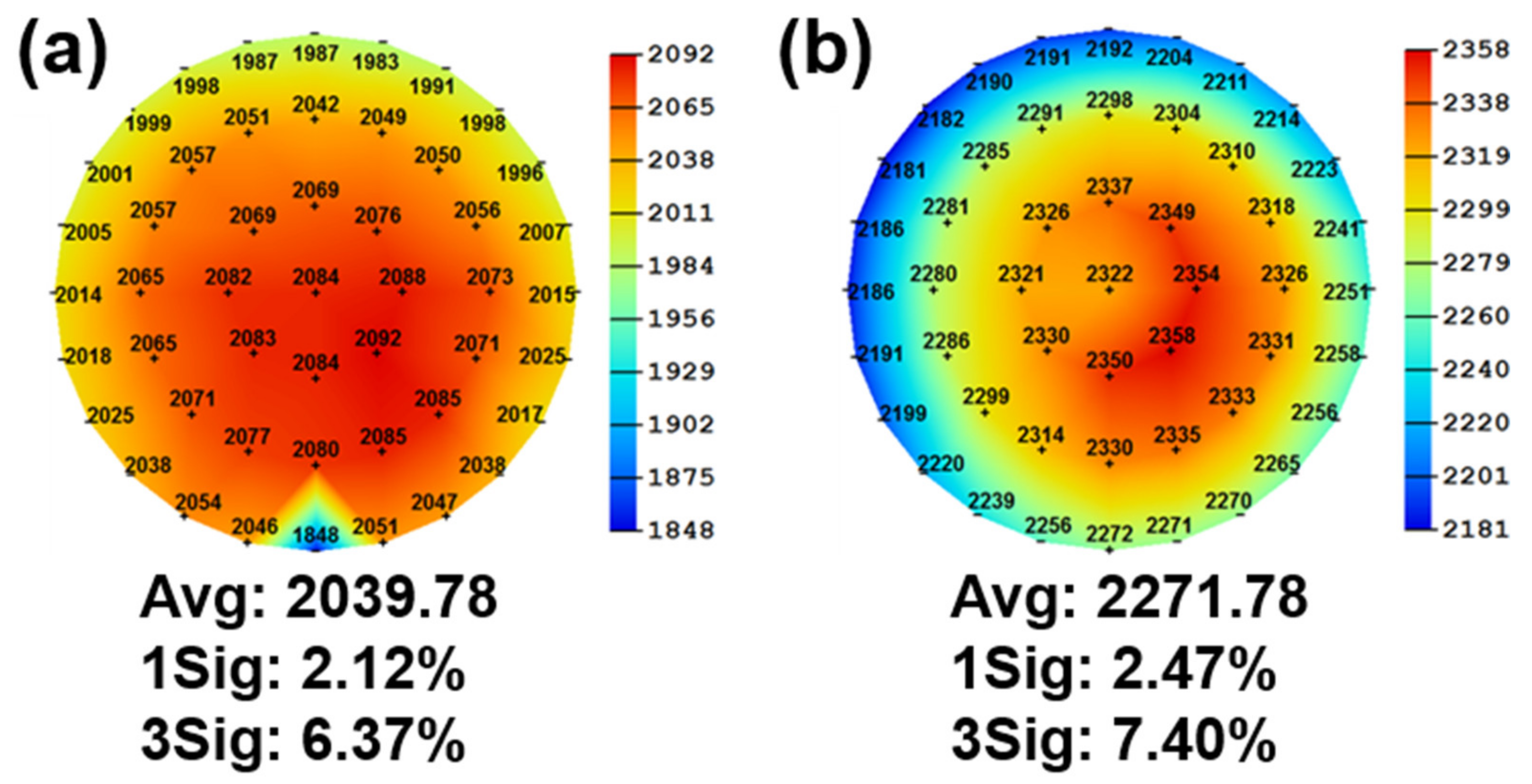
Thickness and elastic modulus are important to define channel hole and to tune etch profile respectively Multiple metrology tools are used to comprehensively characterize this complex system PULSE Acoustic metrology provides thickness and velocity.
. Receiving a substrate on a substrate support in a reaction chamber the substrate comprising the stack and a mask layer that is patterned on top of the stack wherein the stack comprises either a alternating layers of. A method of etching a feature in a stack comprising dielectric material while fabricating a 3D NAND structure the method comprising. Lam Group is exploring the next three to five years as market demand drives memory technologies towards higher density better performance new materials 3D stacking high aspect ratio HAR etch and extreme ultraviolet EUV lithography Production challenges that can be faced providing fab solutions at an economical cost.
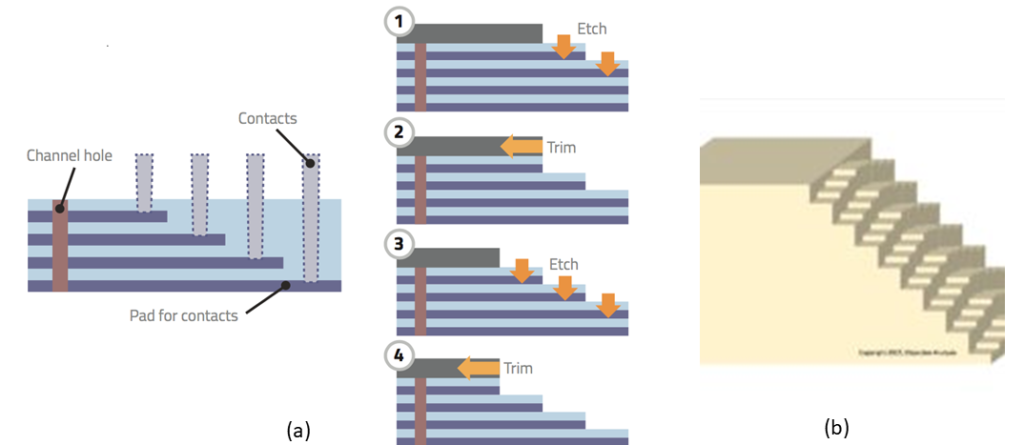
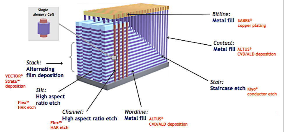
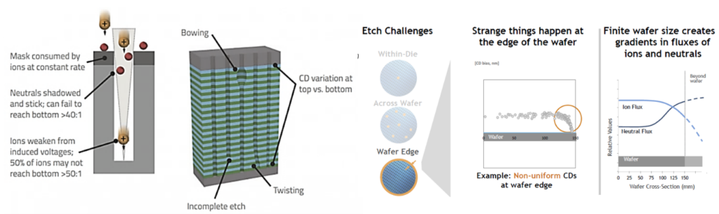
SPE Business Strategy. Creating complex 3D structures with very high-aspect-ration HAR features is complicated and requires extreme precision and ultimately process uniformity and repeatability to achieve scale. Process 10 different contact-hole depths can usually be etched in one etch process and thus four masks and four etch processes are needed to etch all of the contact holes in the staircase and periphery of a 32-cell-stack 3D-NAND flash device.
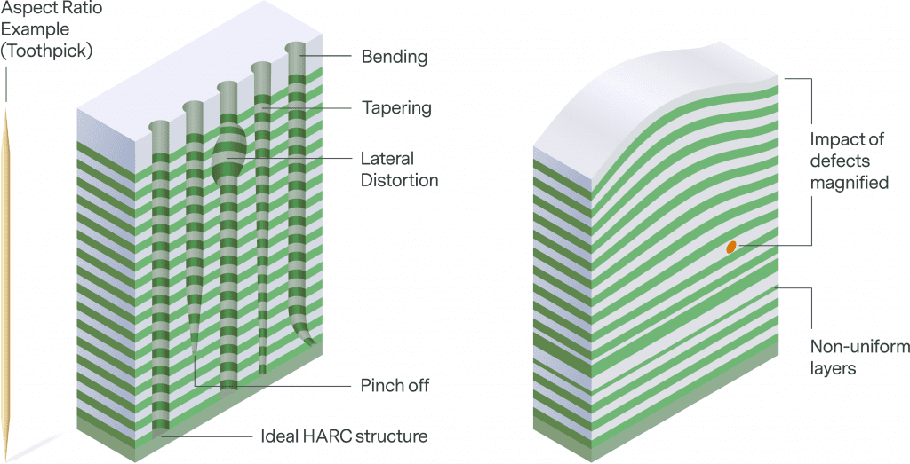
To help visualize this challenge the worlds tallest building the Burj Khalifa in Dubai is 828 m high with a base of 140 m. Read customer reviews find best sellers. Browse discover thousands of brands.
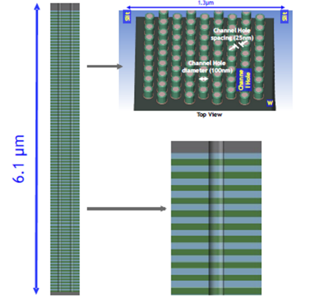
Then an etching process is used to cut a channel through the underlying layers to the substrate. Etching System Achieving success in DRAM as planned. Existing material has to be removed to create the hole.
What is claimed is. A Samsung 3D NAND chip can have up to 25 million such channels. Making these is the problem Once the layer deposition is complete a mask is placed on the top and holes are laid out in it.
Etch Deposition. Continue to Focus on 3D NAND and Logic Word line isolation Slit Multi-level contact DRAM 3D NAND HARC processes Lower customer patterning costs through combining multiple steps into one Improve our position in 9X12X through our clear lead in productivity and etch.

3d Nand Goes Mainstream It Eco Map News Navigator
3d Nand Challenges Beyond 96 Layer Memory Arrays Coventor
2
2

Investigation Of Reducing Bow During High Aspect Ratio Trench Etching In 3d Nand Flash Memory Semantic Scholar
3d Nand Challenges Beyond 96 Layer Memory Arrays Coventor

Nand Market Hits Speed Bump
2

Focus On 3d Nand Manufacturing Challenges An Interview With Entegris I Micronews
3d Nand Challenges Beyond 96 Layer Memory Arrays Coventor

Advanced Memory Solutions Our Solutions Lam Research
Lam Research Rises In Semiconductor Etch Sector On Heels Of 3d Nand Memory Nasdaq Lrcx Seeking Alpha
Process Power The New Lithography Semiconductor Digest

3d Flash Nand Ssd Challenges

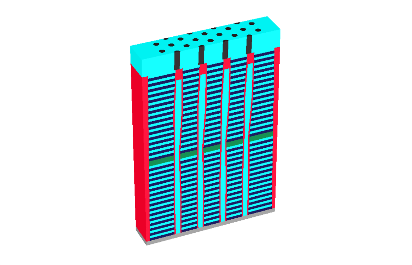
Channel Hole Etch Challenges Lam Research Download Scientific Diagram
Alpha Carbon Hardmask In 3d Nand Device Manufacturing Characterization By Multiple Metrology Methods For In Line Control Of High Aspect Ratio Etching Onto Innovation

Vertical Nand With And Without Tsv A Closer Look I Micronews
Electronics Free Full Text Process Optimization Of Amorphous Carbon Hard Mask In Advanced 3d Nand Flash Memory Applications Html
3d Nand Challenges Beyond 96 Layer Memory Arrays Coventor
